Thickness Monitor FE-3000
- End of Life
- Ongoing Support
|
|
A film thickness measurement system based on the microscopic spectrophotometry features the availability of non-contact and non-destructive measurements with high accuracy and high reproducibility. These systems are widely used in different fields including the semiconductor, flat panel display and other various electronic optical materials.
Are you interested in alliance or distributorship for this product? |
- Product
- Principle
- Specification
- Configuration
- Measured Data
Product
- Light interference thickness monitor for thickness and optical constant analysis of multi layers using reflection spectrum between UV to NIR light.
- Adoption of spectroscopy enables non-contact, non-destructive, highly precise, highly reproducible thickness measurement
- Wide wavelength range(190nm - 1600nm)
- Wide film thickness range (1nm~1mm)
- Microscopic function (Min φ3μm) enables measurement of patterned sample and rough surface sample
- Absolute reflectance
- Film thickness
- Optical constant (n: Refractive index, k: Extinction coefficient)
- Function film, Plastic
Transparent film(ITO, Silver nanowire) Retardation film, Polarization film, AR film,PET,PEN,TAC,PP、PC,PE,PVA, Adhesive, Protect film, Hard coat, - • Semiconductor, Compound semiconductor
Si, oxide film, nitride film, Resist、SiC, GaAs, GaN, InP, InGaAs, Leadframe, SOI, Sapphire - Surface treatment
DLC, Anti-rust, Anti-fog additive - Optical material
Lens, Filter, AR coating - FPD
LCD(CF, ITO, LC, PI, PS), OLED - Others
HDD, Magnetic tape, Construction material
Principle
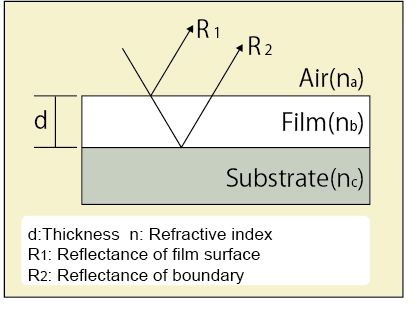
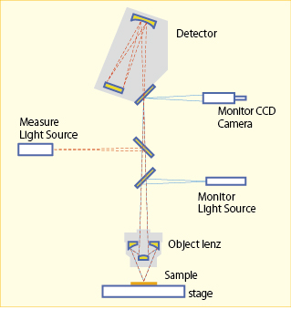
Otsuka Electronics provides non-contact and non-destructive thickness measurements with high accuracy using light interference method and own high performance spectrometer. Light interference method is the optical thickness analysis technique using the reflectance in the spectrophotometer optics. Given an example of the coated film on metal substrate, the beam irradiated from above reflects on the coating surface (R1).Also, transmitted beam reflects on the substrate or boundaries (R2). From the light interference behavior caused by optical path difference and phase shift, film thickness can be calculated using reflectance spectrum and refractive index. Analytical algorisms are Peak-Valley Method, Fast Fourier Transformation (FFT) Method, Non-linear Least-Squares Method and Optimization Method.

Specification
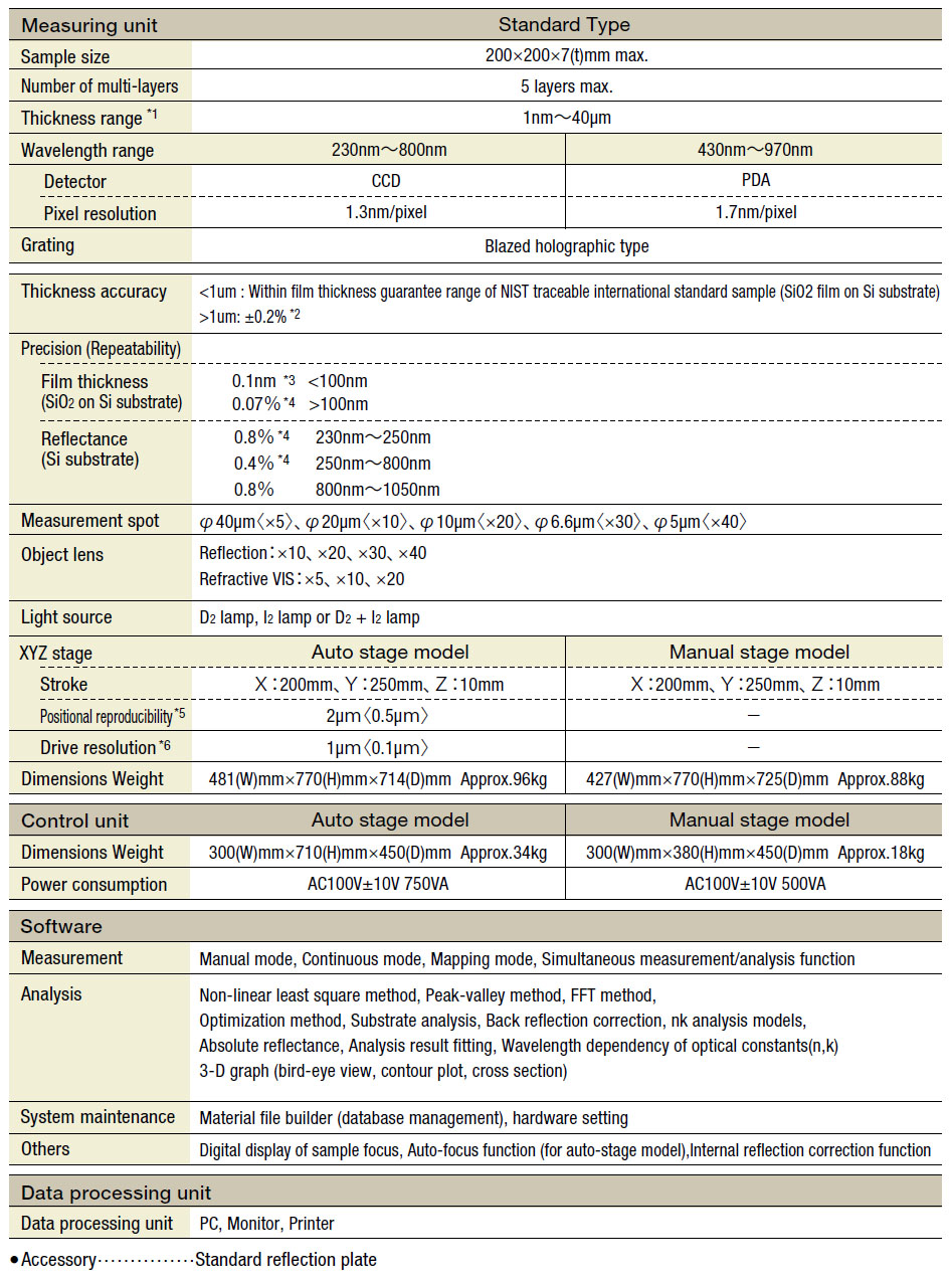
*1: Optical thickness value(n x d). Measurable range depends upon target sample, condition and detector choice.
*2: Calculated value from detector calibration accuracy. Thickness accuracy depends upon target sample.
*3: Expanded uncertainty in repeated measurements at the same point with repeated focusing by means of ×10 reflection object lens and 230nm~800nm model (coverage factor: 2.1)
*4: Relative expanded uncertainty in repeated measurements at the same point with repeated focusing by means of ×10 reflection object lens and 230nm~800nm model (coverage factor: 2.1)×100
*5: Expanded uncertainty in repeated measurements of moving length (coverage factor: 2.1). The value in <> is for micro moving length.
*6: The value in [ ] is for joystick operation.
Configuration

Measured Data
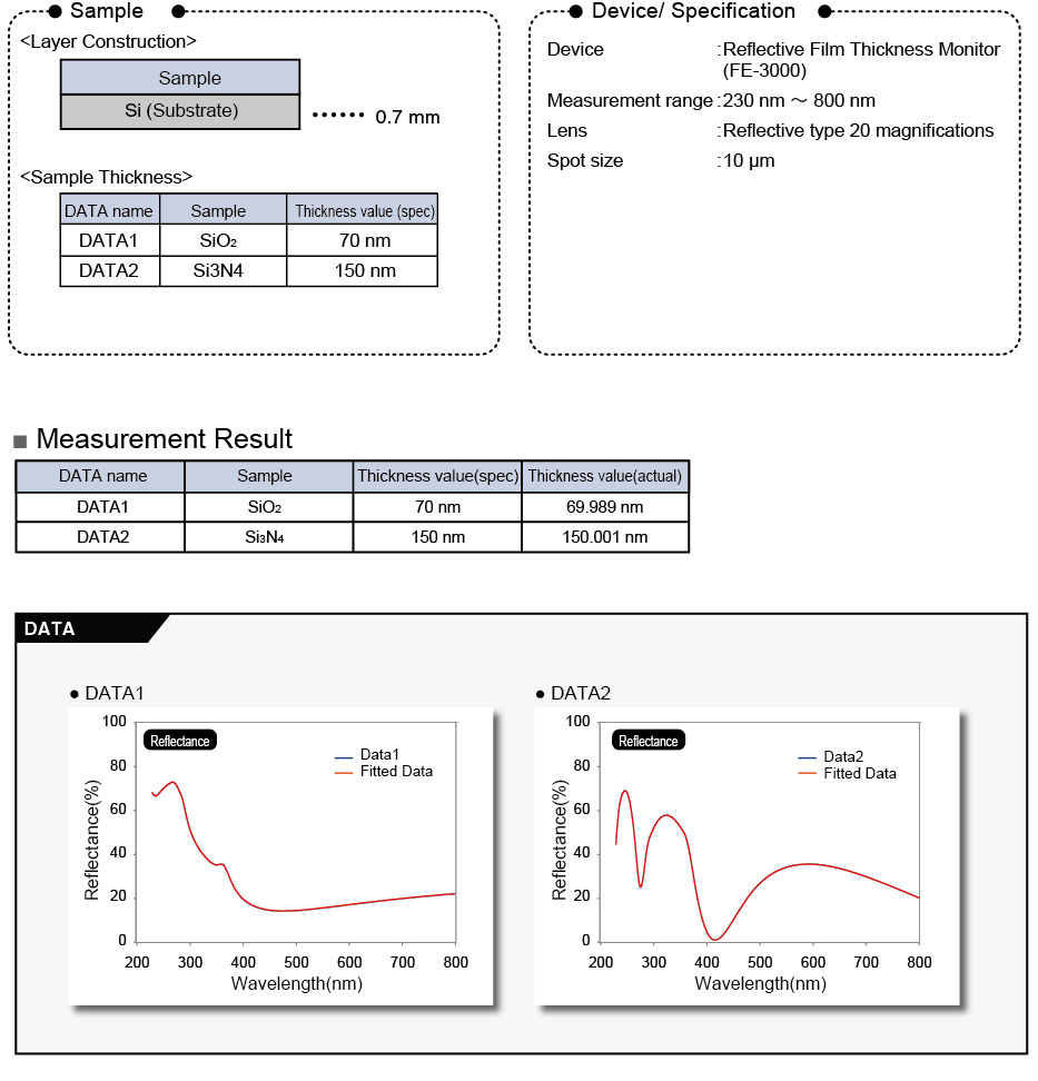
The semiconductor transistor transmits signals by controlling the current conduction state. There is a built-in insulation film in between the transistors to prevent the current leakage and to avoid the accidental current inflow from another transistor. The insulation film is made of SiO2 or SiN. SiN has higher dielectric constant than SiO2 and can be used as a stopper to remove unnecessary SiO2 in CMP. To assess the efficiency as an insulation film and to keep the precise process management, it is mandatory to make a measurement of these film thicknesses.

- Product
- Principle
- Specification
- Configuration
- Measured Data
Related Information
Related Product
|
|
Thickness Monitor FE-300 |
|
|
Array Spectrometer MCPD-9800 |


 Close
Close


